Electron microscopy is an effective method for examining the atomic and molecular structure and characteristics of materials. It includes the creation of high-resolution image of the sample under study using a concentrated beam of electrons.
This method has fundamentally altered the way we perceive the world and helped to make important advances in a wide range of disciplines, from biology to materials science.
History of Electron Microscopy
Max Knoll and Ernst Ruska created the first electron microscope in 1931; for their groundbreaking achievement, they were honored with the 1986 Nobel Prize in Physics. The first type of electron microscope was a transmission electron microscope (TEM), which projects an image onto a fluorescent screen by passing an electron beam through a thin sample.
Since that time, a variety of different electron microscopes have been created, such as scanning electron microscopes (SEM), which offer a detailed 3D view of a sample’s surface, and scanning transmission electron microscopes (STEM), which combine the strengths of TEM and SEM to produce high-resolution images of both surface and internal structures.
Principle of Electron Microscopy
The principle of electron microscopy is the idea that because electrons have a significantly shorter wavelength than visible light, they can discern much tiny characteristics.
- In a TEM, an electron beam is created and directed towards a thin sample that is put on a grid. The sample’s atoms interact with the electrons and scatter or absorb them, resulting in a complicated pattern of diffraction. A high-resolution image of the sample is created by focusing the dispersed electrons onto a fluorescent screen or detector.
- In a SEM, after being exposed to an electron beam and being covered with a thin coating of metal, the sample releases secondary electrons. A comprehensive 3D picture of the sample’s surface is subsequently produced by the detection of these electrons.

Instrumentation of Electron Microscopy
Electron microscopy makes use of cutting-edge equipment to produce and detect electrons. An electron source, lenses for concentrating the electron beam, a sample stage, detectors for sensing electron signals, and computer systems for image processing and analysis make up the primary parts of an electron microscope.
Electron Source
An electron microscope’s electron source is a crucial part. It produces an electron beam that is utilized to photograph the material. The tungsten filament and the field-emission electron source are the two most used types of electron sources. The field-emission electron source generates electrons by delivering a high voltage to a sharp tip, whereas the tungsten filament generates electrons by heating a tungsten wire.
Lenses
The electron beam is focused and controlled using electron lenses. Magnetic lenses are the most popular kinds of electron lenses used in electron microscopy. By bending the electrons’ route using magnetic fields, these lenses concentrate them on the sample. The electron beam may be made to converge or diverge using magnetic lenses, which opens up a variety of imaging options.
Sample Stage
The sample stage secures the sample while enabling accurate placement and movement throughout imaging. To enable imaging of materials at various temperatures, the sample stage of certain electron microscopes may be heated or cooled.
Detectors
Electrons that interact with the sample are found and measured using electron detectors. Scintillators and semiconductor detectors are the two most popular types of electron detectors used in electron microscopy. A photomultiplier detects the photons that scintillators create from the electrons. High sensitivity and resolution are provided by semiconductor detectors, which directly identify electrons.
Computer Systems
The electron microscope is operated by computer systems, which are also utilized to interpret and evaluate the pictures that are produced. The majority of contemporary electron microscopes come with high-end image processing and analysis software, enabling 3D imaging, reconstruction, and other cutting-edge imaging techniques.
In conclusion, electron microscopy instrumentation is intricate and depends on a variety of cutting-edge parts and computer systems. High-resolution imaging of materials and biological samples at the atomic and molecular level is made possible by the cooperative efforts of the electron source, lenses, sample stage, detectors, and computer systems.
Working mechanism of electron microscopy
The working mechanism of electron microscopy involves the following steps:
1. Electron source
A heated tungsten filament or cathode that generates an electron beam serves as the standard electron source. A high voltage, often between 50 and 300 kV, is utilized to accelerate the electrons before they are narrowly focused.
2. Electron lenses
A number of electromagnetic lenses are utilized to focus and steer the electron beam. These lenses perform similarly to the lenses found in a conventional optical microscope, but because of the short wavelength of electrons, they work on a considerably smaller scale.
3. Sample preparation
To endure the high vacuum and electron beam in the microscope, samples must be carefully prepared. Samples must be relatively thin—generally less than 100 nm thick—to for electrons to flow through. While materials science samples are polished and covered with a thin coating of conductive material, biological samples are frequently frozen and sectioned with an ultramicrotome.
4. Interactions with the sample
The electron beam interacts with the atoms in the sample, and this interaction provides information about the sample. There are three main types of interactions:
- Scattering: The atoms in the sample scatter the electron beam, resulting in a diffraction pattern that may be used to identify the sample’s crystal structure.
- Absorption: The sample’s atoms absorb the electron beam, creating a contrast picture that may be utilized to see the sample’s internal organization.
- Emission: The sample may release secondary electrons, backscattered electrons, or X-rays as a result of the electron beam, which can provide details about the sample’s make-up and characteristics.
Detectors and image formation
Different signals are produced by the interactions between the electron beam and the material and are gathered by detectors. The picture of the sample is then created using these signals. Scintillators, fluorescent screens, and CCD cameras are the most often used detectors.
In conclusion, electron microscopy produces and concentrates an electron beam onto a sample to perform its function. As the electrons and atoms in the sample interact, different signals are produced. These signals are gathered by detectors and utilized to build a picture of the sample. Since electron microscopy has such great resolution, it is a crucial technique for imaging at the atomic and molecular scales.
Types of Electron Microscopy
There are several different types of electron microscopy, each with its own unique strengths and limitations. In this article, we will discuss the most common types of electron microscopy.
1. Transmission Electron Microscopy (TEM)
TEM is the most popular kind of electron microscopy, involves sending an electron beam through a thin specimen. The sample’s atoms and electron interactions result in a contrast picture that may be utilized to see the sample’s internal organization. TEM can provide images of structures as tiny as individual atoms and has an incredibly high resolution. It is frequently employed in disciplines including biology, nanotechnology, and materials science.
2. Scanning Electron Microscopy (SEM)
A focused beam of electrons is scanned across the surface of a sample using a scanning electron microscope, or SEM. An image of the sample’s surface may be produced by using detectors to gather the signals that are produced as the electrons interact with the atoms in the sample. SEM may reveal 3D details on the sample’s structure and is especially useful for photographing bigger samples. It is often applied in environmental sciences, forensic investigation, and materials research.
3. Environmental Scanning Electron Microscopy (ESEM)
With ESEM, materials may be imaged in their unprocessed or hydrated states without the requirement for sample preparation. It operates by maintaining a high-pressure atmosphere inside the microscope, enabling the imaging of samples with a lot of water. In the fields of biology, geology, and environmental sciences, ESEM is often used.
4. Scanning Transmission Electron Microscopy (STEM)
STEM uses a concentrated electron beam to scan a thin sample while combining the concepts of TEM and SEM. The signals that are produced as the electrons interact with the sample’s atoms can be captured by detectors and utilized to build a picture of the sample’s internal structure. STEM is frequently employed in the fields of biology and materials research and may enable high-resolution imaging of thin samples.
5. Cryo-Electron Microscopy (Cryo-EM)
Using Cryo-EM, which does not need fixing or staining, it is possible to image materials in their unaltered, hydrated condition. Liquid nitrogen is used to quickly freeze samples while maintaining their original structure. Large and complicated structures, including viruses and proteins, may be imaged with great resolution using cryo-EM technology. In structural biology and drug development, it is frequently used.
Detail on Scanning Electron Microscopy (SEM)
Scanning electron microscopy (SEM) is an imaging tool to analyze the surface of materials at high resolution.
It includes scanning a sample’s surface with an electron beam, creating finely detailed image that show the topography and makeup of the sample.
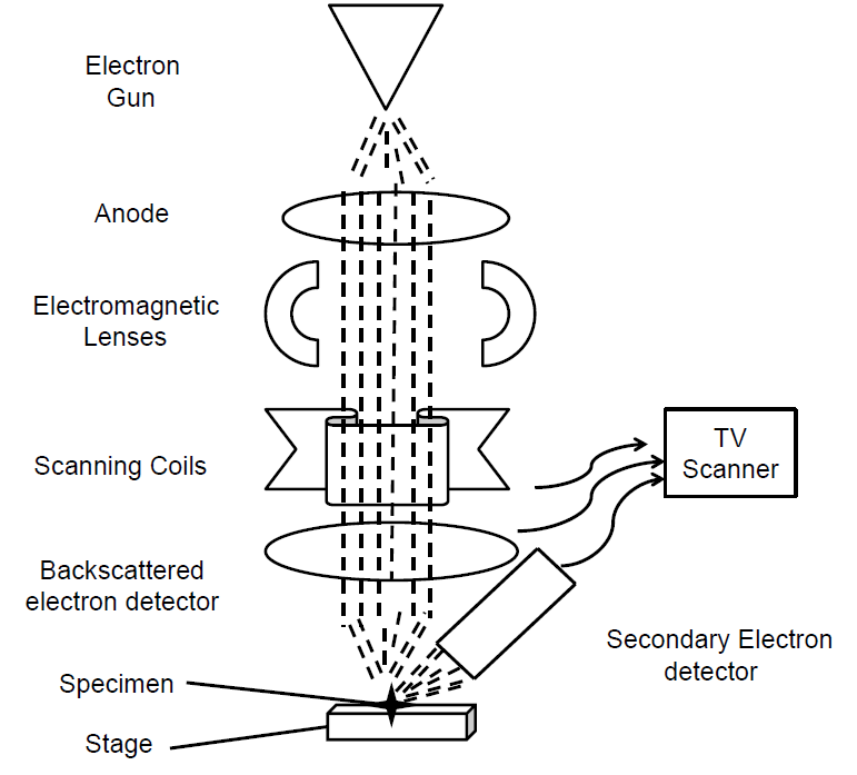
How SEM Works
A SEM generates an electron beam that is directed onto a sample’s surface, which is often coated with a thin coating of metal to improve conductivity. Secondary electrons are released from the sample’s surface as a result of the electrons’ interactions with the sample’s atoms. A detector then picks up these secondary electrons and creates a picture of the sample.
SEM images have the potential to be quite detailed, displaying the sample’s topography down to the nanoscale level. Due to the fact that various components might result in a variety of signals in the detector, images can also provide information regarding the sample’s chemical makeup.
Applications of SEM
SEM is used extensively in the field of materials research to analyze the microstructure and characteristics of materials at high resolution. It is also employed in metallurgy to investigate the surface properties of metals and alloys and comprehend how they behave in various environments.
SEM is used in the area of biology to examine the surface of biological materials, such as cells and tissues, revealing details about their appearance and structure. In order to comprehend how biomaterials and medication delivery systems interact with biological tissues, it is also employed in the research of these topics.
SEM is used in the semiconductor industry for microelectronic quality control and defect investigation. To comprehend the behavior and characteristics of materials at the nanoscale, it is also employed in the study of nanomaterials and nanotechnology.
Detail on Transmission Electron Microscopy (TEM)
Transmission electron microscopy (TEM) is an imaging method used to investigate the atomic and molecular structure and characteristics of materials. It entails the transmission of an electron beam through a thin sample to provide high-resolution pictures of the sample’s interior structure.
TEM has fundamentally changed how we perceive the world and has aided in the development of important new theories in a variety of disciplines, from biology to materials science.
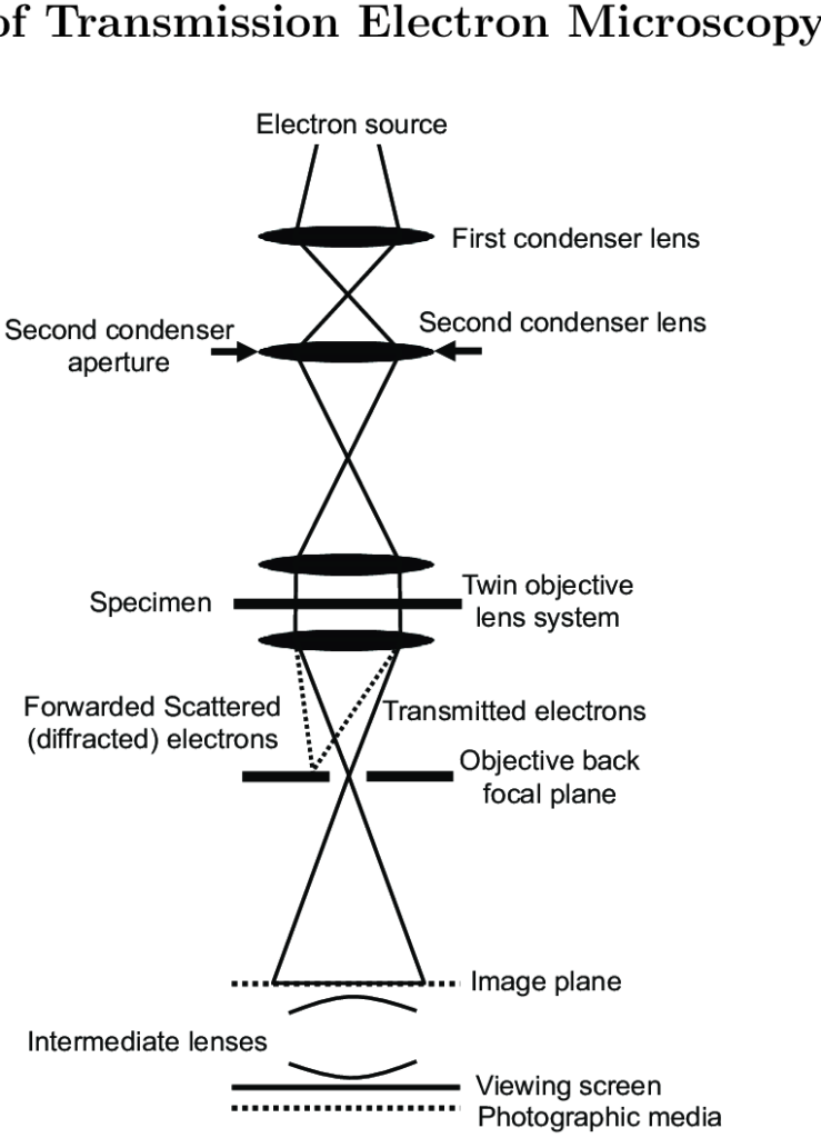
How TEM Works
A TEM generates an electron beam that is focused onto a narrow sample, often one that is less than 100 nanometers thick. The sample’s atoms are affected by the electrons, and a detector on the sample’s other side collects the transmitted electrons.
The sample is then imaged using the transmitted electrons, giving high-resolution details on its interior structure. The crystal structure of materials, the configuration of atoms and molecules, and even the positions of individual atoms, may all be seen in TEM images.
Applications of TEM
In materials research, where it is used to examine the atomic and molecular scales of a material’s microstructure and characteristics, TEM offers a wide range of uses. To research the crystal structure of metals and alloys and comprehend their behavior under various situations, it is also utilized in metallurgy.
In the field of biology, Proteins, nucleic acids, and viruses are only a few examples of the biological molecules whose structure and operation are investigated using TEM. Additionally, it has been used to investigate biological components including mitochondria and ribosomes, shedding light on both their composition and purpose.
TEM is employed in the semiconductor sector as well, where it is utilized to examine the composition and characteristics of microelectronic components like transistors and memory chips.
Differences between Scanning Electron Microscopy (SEM) and Transmission Electron Microscopy (TEM)
| Feature | Scanning Electron Microscopy (SEM) | Transmission Electron Microscopy (TEM) |
| Imaging mode | 2D surface imaging | 2D and 3D imaging of internal structures |
| Resolution | Lower resolution (nanometer to micrometer scale) | Higher resolution (sub-nanometer scale) |
| Sample preparation | Requires coating with a conductive material, no need for thin sections | Requires thin sectioning and staining |
| Sample size | Can image larger samples up to a few centimeters in size | Limited to small samples less than a few millimeters |
| Imaging depth | Shallow depth of field | High depth of field |
| Electron source | Electrons emitted from a tungsten filament or field emitter tip | Electrons emitted from a heated filament or cathode |
| Magnification | Typically, up to 500,000x | Can reach magnifications over 1,000,000x |
| Applications | Material sciences, forensic analysis, environmental sciences, semiconductor industry | Biology, materials sciences, nanotechnology, metallurgy, electronics |

In conclusion, TEM can give high-resolution imaging of interior structures with the necessity for thin sectioning and staining, whereas SEM is best suited for surface imaging of larger samples with lesser resolution. The specific requirements of the experiment and the kind of sample being photographed determine the choice of electron microscopy method.
Future of Electron Microscopy
With continued research and development aiming at enhancing resolution and sensitivity as well as creating new techniques and applications, the future of electron microscopy is bright. Cryo-electron microscopy, which was developed, enables the study of biological molecules in their natural setting without the requirement for fixation or labeling.
In conclusion, electron microscopy has completely changed how we perceive the world around us. It is a fascinating field of microscopic imaging. It has several applications in a variety of sectors and has aided in important scientific breakthroughs. We may anticipate that electron microscopy will become more crucial as technology develops as it helps us understand the world at the atomic and molecular level.